- Home
- News
- Spotlight on Science
- X-ray Bragg holography:...
X-ray Bragg holography: A 3D look inside nanostructures
10-12-2010
The 3D crystal structure of nanoscale materials can be determined using a novel technique involving X-ray Fourier transform holography in Bragg geometry. This method is based on encoding the phase of the scattered wavefield, which bears the information on the internal atomic displacement field of a (nano)structure. The phase information is preserved in the interference of the coherently scattered waves from an object crystal and a small reference crystal. A single inverse Fourier transform of the intensity pattern allows the direct 3D reconstruction of the morphology, density and atomic displacement inside the object crystal of interest. This method opens great possibilities for the investigation of strain fields inside nanostructures.
The complete information on the structure of an object is contained in the electromagnetic field scattered by the object. For decades, efforts have been devoted to holography with coherent visible light [1] in order to reproduce a 3D reconstruction of an object from the intensity pattern only. The strength of the method results from its ability to record the amplitude of the scattered field and to encode the phase in the diffraction pattern, thereby solving the century-old “phase problem”.
Classically, images are produced by lenses, which allow a magnification of the sample, within the resolution limit given by the Rayleigh criterion. However, only the precise knowledge of the complex value of the scattered field can provide the detailed and correct image of the sample. Therefore, the application of lens-less imaging techniques has earned much attention recently. X-ray techniques – with a wavelength within the angstrom range – are particularly useful for nanoscience, where detailed knowledge of the internal structure on the nanoscale is of fundamental importance to understand and reveal the nanostructure’s physical properties. Several examples of holography with X-rays have been reported in the literature [2], performed in the forward direction geometry (i.e. near the origin of the reciprocal space) practically restricting the imaging to two dimensions.
In this work we have used the advantages offered by the Bragg geometry (i.e. when the measurement is performed in the vicinity of one of the Bragg points). Easy access to the 3D diffraction intensity pattern provided by the Bragg geometry allows a generalisation of the X-ray holography method to the 3D case. Fourier transform holography [3] makes use of the interference produced between the field scattered by the sample, referred to as the object crystal and a small reference crystal located near the object of interest, i.e. within the coherence length of the incident X-ray beam. The sample image is obtained by a single inverse Fourier transform of the far-field intensity pattern rendering a real space image of the sample. In addition to the 3D benefit, Bragg geometry is also sensitive to the displacement field in the crystal. Therefore Bragg Fourier transform holography is an attractive alternative to coherent diffraction imaging which is based on computing resources and hungry iterative algorithms, and which fails so far to address the highly inhomogeneous strain field case. This is a point of major interest as non-destructive measurements of the 3D displacement field at the nanoscale are still challenging [4].
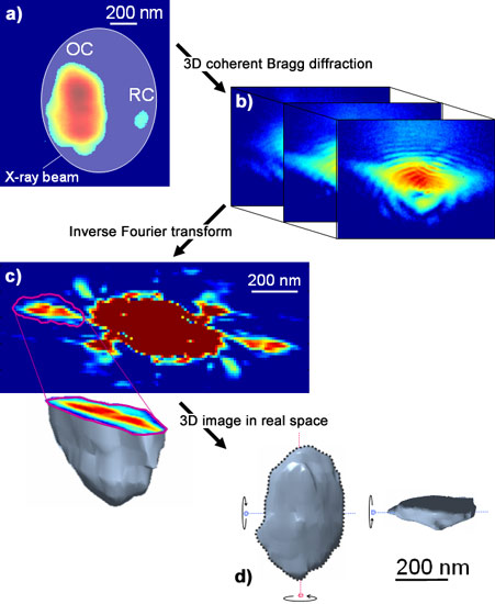
The sample used for this work consisted of an object crystal and a small reference crystal (see the AFM image in Figure 1a) produced by e-beam lithography from a SiGe continuous layer (200 nm thick). The experiment was carried out at beamline ID01. To increase the flux on the sample, a coherently illuminated Fresnel zone plate was used, which produces a focused coherent beam. The 3D coherently scattered intensity around the SiGe (004) Bragg peak was measured by a Maxipix detector for different values of the rocking angle. A typical 2D slice (one detector frame) is shown in Figure 1b. The low and high frequency fringes result from the interference of the waves scattered from the two crystals and are induced by their small and finite size. These slices are stacked in a 3D matrix for the inversion process: after a single inverse Fourier transform, the 3D sample image is retrieved in a straightforward manner (Figure 1c).
The three-dimensional shape views shown in Figure 1d agree with the sample topology obtained from AFM measurements. More interesting is the internal view of the sample structure, which demonstrates the capability of the method to give access to the 3D description of the sample electron density and the displacement field (for details see principal publication).
The simplicity and robustness of the inversion using Bragg Fourier transform holography paves the way to in situ investigations of inhomogeneous strain fields in nanocrystals and thus will be beneficial to the understanding of current strain related problems in nanomaterial research.
Acknowledgement
This work was funded by the French ANR (ANR-08-JCJC-0095-01) and the FWF Vienna (SFB025).
References
[1] D. Gabor, W.E. Kock, and G.W. Stroke, Science 173, 11 (1971).
[2] S. Eisebitt et al., Nature (London) 432, 885 (2004); L.-M. Stadler et al., Phys. Rev. Lett. 100, 245503 (2008).
[3] G.W. Stroke and D. Falconer, Phys. Lett. 13, 306 (1964); J.T. Winthrop and C.R. Worthington, Phys. Lett. 15, 124 (1965).
[4] A. Diaz, et al., New J. Phys. 12, 035006 (2010).
Principal publication and authors
V. Chamard (a) J. Stangl (b) G. Carbone (c), A. Diaz (c), G. Chen (b), C. Alfonso (d), C. Mocuta (c), and T.H. Metzger (c), Three-Dimensional X-Ray Fourier Transform Holography: The Bragg Case, Phys. Rev. Lett. 104, 165501 (2010).
(a) Institut Fresnel, CNRS, Aix-Marseille University, Marseille (France)
(b) Institute of Semiconductor and Solid State Physics, Johannes Kepler Universität, Linz (Austria)
(c) ESRF
(d) IM2NP, CNRS, Aix-Marseille University, Marseille (France)


