- Home
- News
- Spotlight on Science
- Multi quantum well...
Multi quantum well electroabsorption-modulated laser characterised by hard X-ray microprobe
12-05-2010
A multi quantum well electroabsorption-modulated laser is a semiconductor device employed in long-distance, high-frequency optical-fibre communication. The most advanced devices involve monolithic integration of two functions, electroabsorption modulator and distributed feedback laser, at the chip level. Devices are manufactured by state-of-the-art methods of substrate masking and vapour deposition, but the results of this process are judged empirically. Here scientists have used an ESRF hard X-ray microprobe to characterise the semiconductor material constituents of such a device with unprecedented detail.
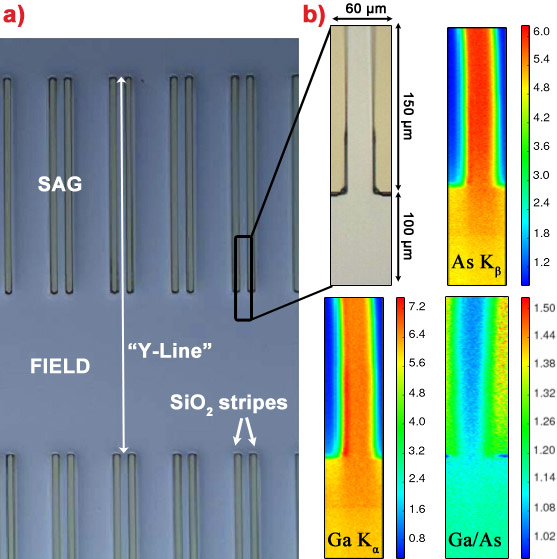
Multi quantum well (MQW) electroabsorption modulated lasers (EML) are widely used in optical communication systems. MQW structures are based on quaternary III-V semiconductor alloys deposited on suitable substrates. High performance optoelectronic devices require monolithic integration of different functions at chip level. Excellent results in the development of monolithic integration have been reached with the selective area growth (SAG) technique [1]. SAG exploits the perturbation of the growth fluxes induced by a dielectric mask (usually SiO2): when the metallorganic precursors collide with the dielectric mask, they are deflected and they can desorb or migrate through the unmasked semiconductor where the growth can start. In this way the reactive species coming from the gas phase are enriched by those deflected by the mask and a different material is obtained with respect to the unmasked region. Since the reactive species have different diffusion lengths [2], the result is a variation in composition and thickness of semiconductors grown near (SAG region) and far (field region) from the mask (Figure 1a).
 |
|
Figure 1. a) Optical micrograph of the SiO2 stripe-patterned InP substrate allowing SAG growth. The black rectangle, magnified in part b), shows the region sampled in the XRF maps. b) Spatial maps of the fluorescence counts of the principal element’s lines (beam energy 17 keV). The last map shows the ratio between Ga(Kα) and As(Kβ) counts highlighting the change in the average (well plus barrier) AlxGayIn1-x-yAs quaternary composition in the SAG region. The fluorescence is scaled in arbitrary units. |
One of the most promising applications of SAG is EML [3] obtained by monolithic integration of an electroabsorption modulator (EAM) with a distributed feedback laser. A voltage modulation at 10 GHz applied to the EAM switches it between an opaque and a transparent state by means of the Stark effect [4] and ensures the modulation of the laser emission, allowing long-distance communications (up to 80 km) at high frequency (10 Gb/s). The SAG EML device investigated in the present work is an AlxwGaywIn1-xw-ywAs/AlxbGaybIn1-xb-ybAs (compressive-strained well/tensile-strained barrier) MQW structure grown on InP by metallorganic vapour phase epitaxy. The SAG mask used for the growth (Figure 1a) featured 20 μm wide SiO2 stripes with a 30 μm opening width between them.
Figure 1b shows the results of X-ray fluorescence (XRF) mapping at beamline ID22: the maps reveal that Ga Kα and As Kβ counts are higher in the SAG region owing to material enrichment caused by the SiO2 stripes. The effectiveness of the SAG technique in modulating the chemical composition of the quaternary alloy is proven by the map reporting the ratio between Ga and As counts in which a gradient in the average well/barrier chemical composition is clearly visible. Since the Ga/As ratio is lower in the SAG region than in the field, we can assert that the average Ga content of the MQW structure progressively increases by moving from the SAG to the field in the middle of a couple of stripes (along the region labelled “Y-line” in Figure 1a). This is due to the SAG effect that exploits the shorter effective diffusion length (D/k) of In with respect to that of Ga and Al [2].
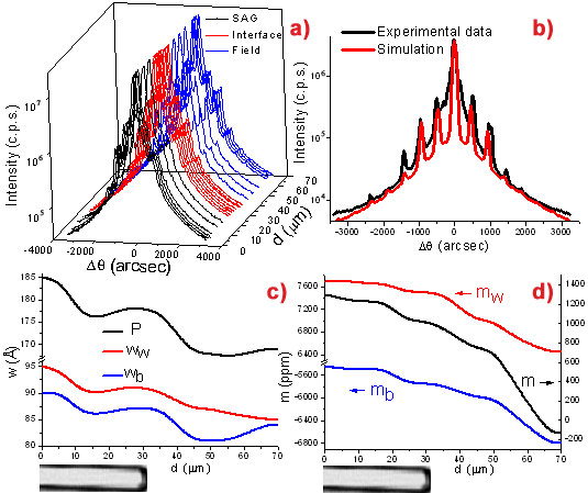
The structural parameters of the sample were investigated by µ-X-ray diffraction (µ-XRD): 35 different spatial points were sampled along the Y-line (Figure 2a). With such data, it is possible to obtain the width (wb, ww, Figure 2c) and the mismatch (mb, mw, Figure 2d) of the barrier and of the well by fitting the observed pattern [5,6] using a model based on the dynamic theory of X-ray diffraction (Figure 2b). It is possible to see that wb and ww undergo a modulated increase moving from field to SAG regions: this is the direct measure of the material enrichment in the SAG region. Moreover, both mb and mw values increase almost monotonically moving from the field to the SAG region, reflecting the expected modulation of the AlxGayIn1-x-yAs composition of barrier and well layers, that makes possible two MQW heterostructures with two different functions monolithically integrated in the same epitaxial growth.
 |
|
Figure 2. a) Selection of some of the 35 full X-ray diffraction patterns collected along the Y-line starting 30 μm before the end of the stripes in the SAG region. b) Example of comparison between experimental and simulated XRD patterns in the field region. c) Barrier and well widths and period as a function of the position along the Y-line, obtained by simulation of the 35 experimental XRD patterns (the image at the bottom shows the location of the masked region). d) As part c) for the well, barrier and overall mismatches. |
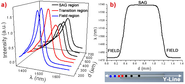
This key information, coupled with the μm-determination of the energy gap (Figure 3) allows us to understand the structural gradient of the MQW structure along the Y-line from the field to the SAG region. The µm-space resolved photoluminescence study, reported in Figure 3, also highlights that the distributed feedback laser (SAG region) emits at the desired wavelength for third window communications (l = 1.55 µm) and that the EAM (field region) has a higher energy gap. The latter point implies that the modulator is transparent to the radiation emitted by the laser, when the negative potential is not applied.
 |
|
Figure 3. a) Selection of seven (out of 100) photoluminescence spectra collected along a 1500 μm-long Y-line covering the complete mask from field to field. b) Top: maximum of the emission for each spectrum vs. position along the Y-line. Bottom: optical micrograph correlating the photoluminescence maximum (top) with the position on the sample. The seven coloured points highlight the positions where the full spectra reported in a) were collected. |
This unprecedented characterisation allowed us to determine the structure of the grown heterostructure with a monolayer-resolution (~ 5 Å) along the growth axis and with μm-resolution in the growth plane. This knowledge yields the appropriate feedback needed to improve the growth process, previously based only on a trial/error approach. A new generation of devices may arise by applying this method to other SAG growths with different stripes and opening sizes [7].
References
[1] A.M. Gibbon, J.P. Stagg, C G. Cureton, et al., Semicond. Sci. Technol. 8, 998 (1993).
[2] J. Decobert, N. Dupuis, P.Y. Lagree, et al., J. Cryst. Growth 298, 28 (2007).
[3] R.A. Salvatore, R.T. Sahara, M.A. Bock, and I. Libenzon, IEEE J. Quantum Electron. 38, 464 (2002).
[4] D.A.B. Miller, D.S. Chemla, and T.C. Damen, Phys. Rev. Lett. 53, 2173 (1984).
[5] C. Lamberti, Surf. Sci. Rep. 53, 1 (2004).
[6] C. Ferrari and C. Bocchi, in Characterization of Semiconductor Heterostructures and Nanostructures, edited by C. Lamberti (Elsevier, Amsterdam, 2008), p. 93.
[7] L. Mino, A. Agostino, S. Codato and C. Lamberti, J. Anal. At. Spectrom. 25, 831-836 (2010).
Principal publication and authors
L. Mino (a), D. Gianolio (a), G. Agostini (a), A. Piovano (a), M. Truccato (b), A. Agostino (c), S. Cagliero (c), G. Martinez-Criado (d), S. Codato (e) and C. Lamberti (a), Structural Characterization of Multi-Quantum Wells in Electroabsorption-Modulated Lasers by using Synchrotron Radiation Micrometer-Beams, Adv. Mater. 22, 2050–2054 (2010).
(a) Department of Inorganic, Materials and Physical Chemistry, University of Turin (Italy)
(b) Department of Experimental Physics, University of Turin (Italy)
(c) Department of General and Organic Chemistry, University of Turin (Italy)
(d) ESRF
(e) Avago Technologies Italy S.r.l., Turin (Italy)
Top image: Characterisation of a laser/modulator device using the ESRF hard X-ray microprobe.
partners


European Synchrotron Radiation Facility - 71, avenue des Martyrs, CS 40220, 38043 Grenoble Cedex 9, France.