- Home
- News
- Spotlight on Science
- Scanning X-ray diffraction...
Scanning X-ray diffraction with 200 nm spatial resolution
11-08-2008
Strongly-collimated monochromatic X-rays enable nanodiffraction with both a very high, sub-micrometre resolution in real space and high angular resolution in reciprocal space. Individual and clearly distinguishable shape features of a single object could be examined for the example system of self-organised SiGe/Si Stranski-Krastanow islands.
A variety of experimental methods at synchrotron sources require small and intense X-ray beams. This is particularly true for coherent scattering techniques and X-ray microtomography. When using hard X-rays, most materials are optically thinner than vacuum, this is related to a real part of the diffraction index being slightly smaller than unity - about 0.9999. Consequently, a single X-ray refractive lens will yield a rather large focal length and thus compounds of many lenses have been developed for this purpose [1]. Great advances have been made towards decreasing spot sizes down to 50 nm using refractive optics during the last few years [2], in particular at third-generation synchrotron sources such as the ESRF and in the near future at PETRA III (Hamburg, Germany). Furthermore, the increasing demand for sub-µm focussed hard X-rays has the benefit of driving applications as well as the improvement of common techniques.
We have developed a scanning technique that combines high-resolution X-ray diffraction (in reciprocal space) along with a sub-µm spatial resolution (in real space). The model system used to check the limits of the method was SiGe/Si(001) Stranski-Krastanow islands. A set of refractive silicon X-ray lenses focussed the X-ray beam size down to a diameter of 200 nm (FWHM), which enables scanning of individual µm-sized or smaller islands. By illuminating diverse {111} island side facets, crystal truncation rods of different orientation were independently excited and thus became distinguishable in the scattering patterns. The re-assembly of these locally-resolved diffraction patterns coincides with both an integral measurement and a corresponding scattering simulation.
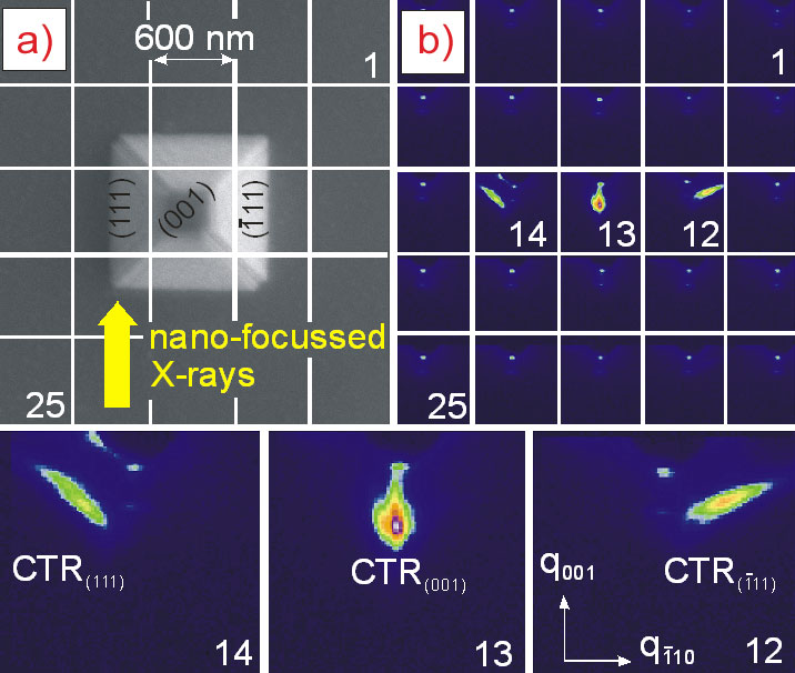
Figure 1a presents the local scan range for the structure under investigation. An area of 3x3 µm2 around a single SiGe/Si(001) island (1.2 µm base width) was divided into a grid of 5x5 measuring points, each with a 1 second exposure time. At each of these locations, the diffusely scattered intensity near the symmetric (004) reflection was recorded with a CCD (FReLoN) system (pixel size 50 µm) placed 500 mm behind the sample. Figure 1b gives corresponding slices of the reciprocal space closely around the island reflection. Please note that each image exhibits a highly-resolved diffraction pattern, indicating that individual island regions have been probed.
 |
|
Figure 1. a) Scanning electron micrograph of a typical SiGe/Si(001) island confined by four {111} side and a single (001) top facet. An area of 3x3 µm2 was symmetrically divided into 25 points, where shape and strain have been locally probed with a monochromatic 200 nm X-ray spot. b) Frames 1-25 of the scanning X-ray diffraction micrograph give the diffusely scattered X-ray intensity near the symmetric Si(004) reflection, which itself has been suppressed by an absorber. If the incoming X-ray beam subsequently illuminates different {111} island facets, the corresponding facet rods will be excited and thus contribute to the scattering pattern frame (12-14). |
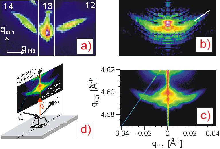
On the base of a so-called kinematical scattering approach, the respective X-ray diffraction patterns can be simulated while using the three-dimensional deformation field derived by a finite element method (For more details of this method see, e.g., [3]). It is reasonable to presume that islands can elastically relax during the growth sequence - a confirmed result for a broad variety of heteroepitaxial systems. This indicates an increasing germanium content towards the island apex [4]. Figure 2b gives an improved X-ray simulation of an entire island consisting of 12% germanium at the lower third and 14% above. Since the silicon substrate has been omitted for the scattering simulation itself, just the butterfly-like feature due to the island becomes visible. The guiding white line gives the nominal direction of one of the {111} facet rods.
 |
|
Figure 2. a) The re-assembled diffraction pattern of a single island; b) a simulated diffraction pattern; c) an integral measurement averaging over an ensemble of islands. d) The setup depicts schematically the diffraction plane (defined by the wave vectors ki and kf) with respect to the island orientation. |
Figures 2b and 2c refer to entire islands, whereas the frames in Figure 1b show locally-resolved X-ray diffraction patterns with a sub-µm, hence sub-island step width. Individually illuminated {111} facets (there are four) excite differently inclined facet rods (denoted 12, 13 and 14) in the enlarged frames. Obviously the nano-focussed X-rays probe each part of the island as a kind of semi-infinite crystal. Please note that only two of the overall four facet rods are visible in the given slice due to the fact that two rods (which one may expect to be located directly above and below frame 13) occur in a perpendicular plane. Finally, the re-assembled diffraction pattern in Figure 2a fits well with the X-ray simulation and the integral measurement. This method has the invaluable advantage of being able to probe objects individually. Hence the proposed technique serves regardless of non-uniformity throughout an island ensemble. Further to the work described here, we have mapped at each position an entire three-dimensional reciprocal space map (not shown here) near the (004) reflection. Thereby we have probed the local strain distribution within different islands areas, and this will be the subject of a future publication.
References
[1] A. Snigirev, V. Kohn, I. Snigireva, B. Lengeler, Nature 384, 49 (1996).
[2] C.G. Schroer, B. Lengeler, Phys. Rev. Lett. 94, 054802 (2005).
[3] M. Hanke, M. Schmidbauer, D. Grigoriev, H. Raidt, P. Schäfer, R. Köhler, A.-K. Gerlitzke, H. Wawra, Phys. Rev. B 69, 075317 (2004).
[4] C. Mocuta, J. Stangl, K. Mundboth, T.H. Metzger, G. Bauer, I. Vartanyants, M. Schmidbauer, T. Boeck, ESRF Highlights 2007, p.85.
Principal publication and authors
M. Hanke (a), M. Dubslaff (a), M. Schmidbauer (b), T. Boeck (b), S. Schoeder (c), M. Burghammer (c), C. Riekel (c), J. Patommel (d), C.G. Schroer (d), Scanning x-ray diffraction with 200 nm spatial resolution, Appl. Phys. Lett. 92, 193109 (2008).
(a) Martin-Luther-University Halle-Wittenberg, Halle/Saale (Germany)
(b) Leibniz Institute for Crystal Growth, Berlin (Germany)
(c) ESRF
(d) Technical University, Dresden (Germany)
Related content
Beamline ID13: http://www.esrf.eu/UsersAndScience/Experiments/SCMatter/ID13/
partners


European Synchrotron Radiation Facility - 71, avenue des Martyrs, CS 40220, 38043 Grenoble Cedex 9, France.